Can three-dimensional printing achieve precise micro-scale details in copper components?
Can 3D Printing Achieve Precise Micro-Scale Details in Copper Components?
Resolution Limits of Copper 3D Printing Technologies
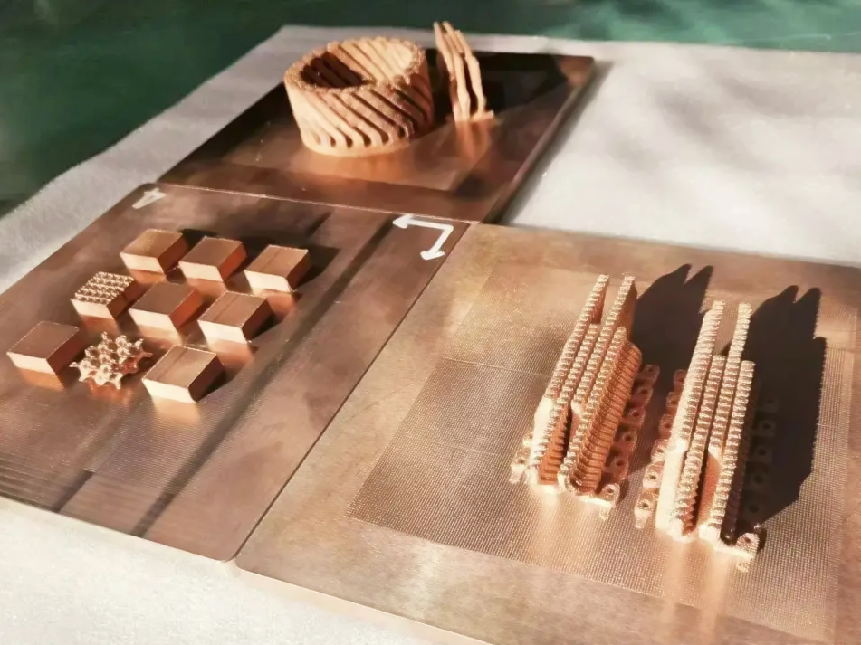
Achieving micro-scale precision in copper components via 3D printing is feasible, especially with high-energy density processes like Direct Metal Laser Sintering (DMLS) and Electron Beam Melting (EBM). These technologies support layer thicknesses of 20–40 µm and laser spot sizes as small as 80–100 µm, making them suitable for fine copper features such as high-aspect-ratio channels, thin walls, and fine lattice structures.
Design Considerations for Fine Copper Features
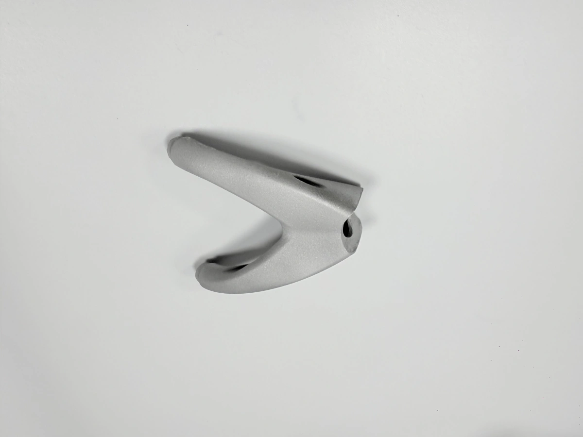
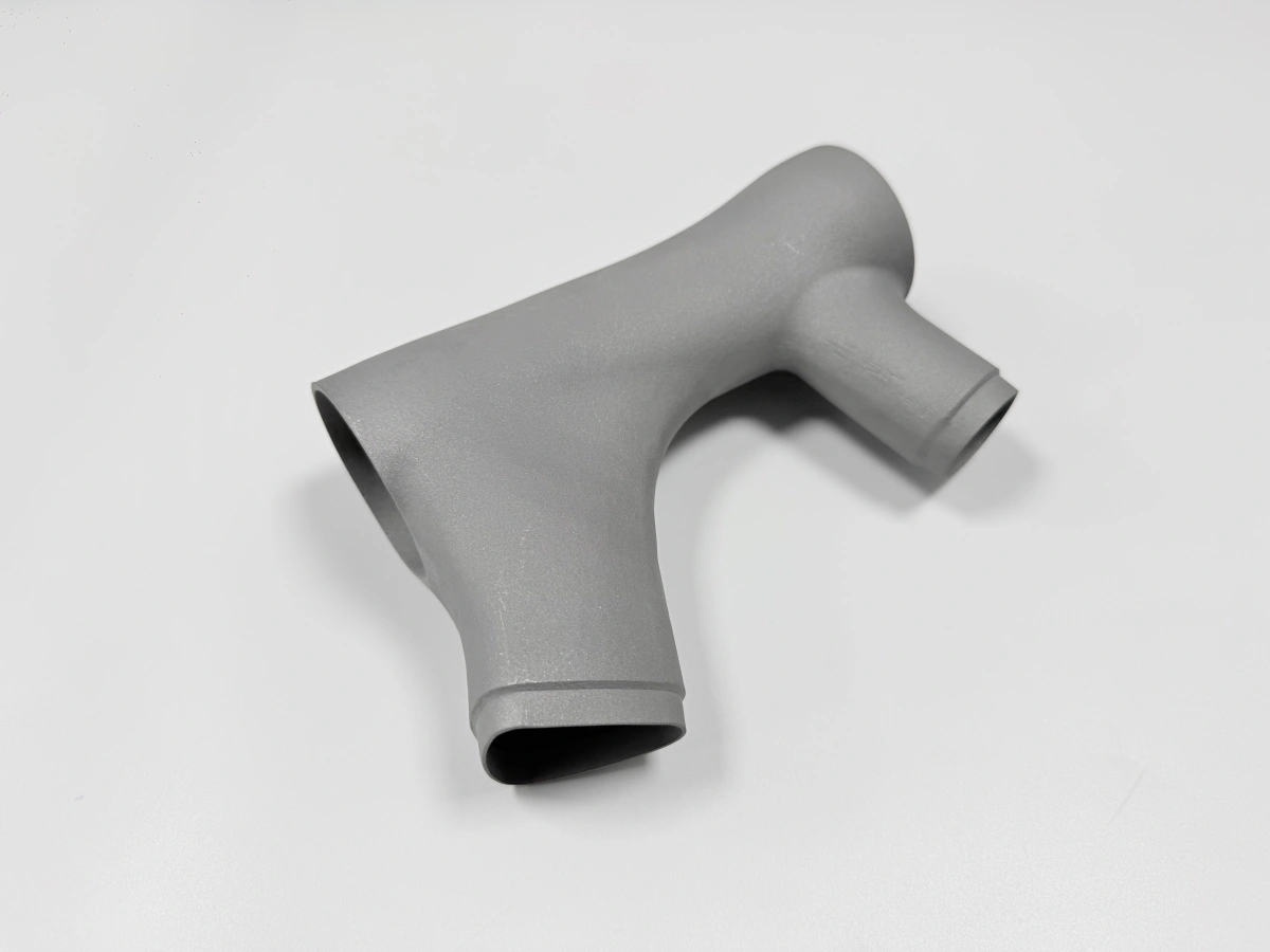
Due to copper’s high reflectivity and thermal conductivity, laser absorption is less efficient compared to other metals. To counteract this, Neway employs customized print parameters and powder morphology optimization when printing high-purity Copper C101 or Pure Copper. Minimum wall thicknesses of 150–200 µm and hole diameters down to 300 µm can be achieved with repeatable tolerances, suitable for RF antennas, microchannel cold plates, and power connectors.
Surface Quality and Post-Processing
Although native surface roughness for printed copper parts typically ranges from Ra 8–15 µm, this can be significantly improved using post-processing methods. Electropolishing and precision CNC machining allow finishing to Ra < 1 µm for critical interfaces. Dimensional tolerances can be refined to ±0.05 mm or better after finishing.
Application Examples
Neway frequently delivers high-precision copper parts for industries such as consumer electronics, aerospace, and medical devices. Common micro-scale components include microchannel heat sinks, precision RF waveguides, and miniaturized electromagnetic shielding enclosures.
Recommended Micro-Detail Copper Printing Services from Neway
High-Resolution Copper Printing: Produce intricate geometries with Copper C110, GRCop-42, and CuCr1Zr using optimized DMLS or EBM platforms.
Surface Refinement Solutions: Improve micro-feature accuracy and finish through CNC machining, HIP, and surface treatment processes like electropolishing and coating.
Engineering Consultation for Critical Features: Receive tailored DfAM support for micro-scale thermal, electrical, and mechanical copper parts across electronics, aerospace, and energy industries.