Copper C101
Introduction to Copper C101 for 3D Printing
Copper C101, also known as oxygen-free high-conductivity (OFHC) copper, contains a minimum of 99.99% pure copper. It offers outstanding electrical conductivity (>100% IACS), high thermal conductivity (391 W/m·K), and excellent ductility, making it ideal for RF components, busbars, thermal sinks, and advanced electronics.
Using precision methods like Direct Metal Laser Sintering (DMLS) and Electron Beam Melting (EBM), Copper C101 achieves dimensional tolerances of ±0.1 mm while retaining superior thermal and electrical properties.
International Equivalent Grades of Copper C101
Country | Grade Number | Other Names/Titles |
|---|---|---|
USA | C10100 | OFHC Copper |
Europe | CW008A | EN 13601 |
UK | C101 | BS EN 12163 |
Japan | C1011 | JIS H3100 |
China | TU0 | GB/T 5231 |
Comprehensive Properties of Copper C101
Property Category | Property | Value |
|---|---|---|
Physical | Density | 8.94 g/cm³ |
Melting Point | 1,083°C | |
Thermal Conductivity | 391 W/m·K | |
Electrical Conductivity | >100% IACS | |
Chemical | Copper (Cu) | ≥99.99% |
Oxygen (O₂) | ≤0.0005% | |
Mechanical | Tensile Strength | 220 MPa |
Yield Strength | 70 MPa | |
Elongation | ≥30% | |
Hardness (Vickers HV) | ~50 HV |
Suitable 3D Printing Processes for Copper C101
Process | Typical Density Achieved | Surface Roughness (Ra) | Dimensional Accuracy | Application Highlights |
|---|---|---|---|---|
≥99% | 10-14 µm | ±0.1 mm | Enables fine-featured thermal and RF components with high electrical conductivity | |
≥99.5% | 20-30 µm | ±0.15 mm | Suitable for high-mass thermal management parts with excellent material purity |
Selection Criteria for Copper C101 3D Printing Processes
Conductivity Requirements: DMLS ensures over 95% IACS in printed form, ideal for waveguides, antenna components, and high-frequency connectors.
Part Size and Geometry: EBM is suitable for thicker geometries and high-volume thermal blocks; DMLS handles finer details for intricate electrical circuits.
Surface Finish Tolerance: Post-machining and polishing may be required to reduce Ra < 1 µm for high-performance electrical contact surfaces.
Post-Processing Necessity: Heat treatments may be applied to improve grain structure and conductivity post-printing without compromising precision.
Essential Post-Processing Methods for Copper C101 3D Printed Parts
CNC Machining: Used to refine surfaces and tolerances to ±0.02 mm for thermal interfaces and precise mounting geometries.
Electropolishing: Improves electrical contact and reduces surface roughness to <0.5 µm Ra for RF and electronic parts.
Heat Treatment: Conducted at ~400°C for 2 hours in a controlled atmosphere, enhancing conductivity and relieving internal stresses.
Tumbling: A mechanical finish to deburr and smooth external surfaces, ensuring optimal fit and surface functionality.
Challenges and Solutions in Copper C101 3D Printing
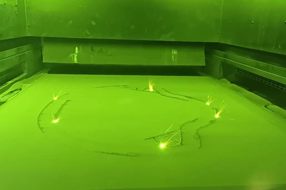
High Reflectivity: Laser absorption is low; optimized green laser technology or electron beams improve melting stability and density.
Thermal Conductivity: High conductivity leads to rapid heat dissipation; adjusted scan strategies maintain uniform melt pools.
Oxidation Sensitivity: Printing in inert argon or vacuum chambers prevents oxidation, preserving electrical and mechanical performance.
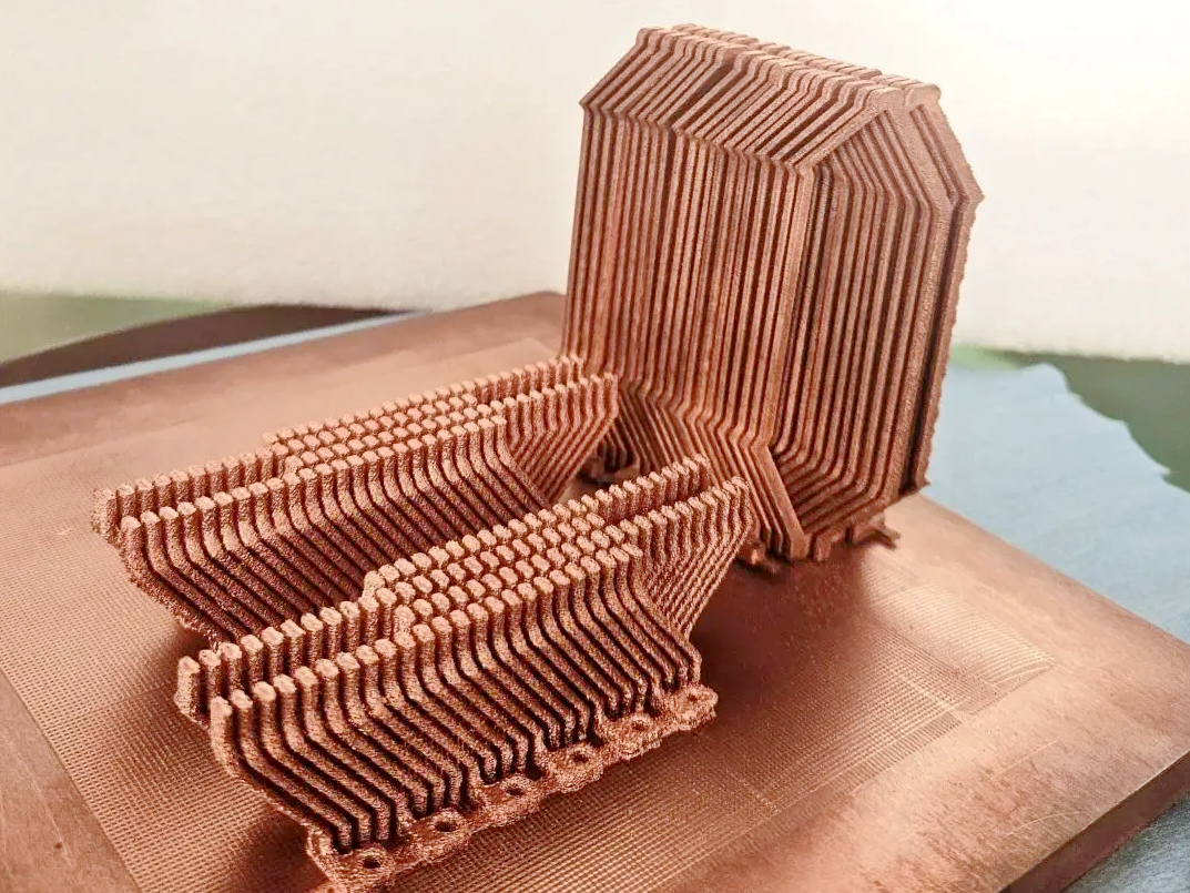
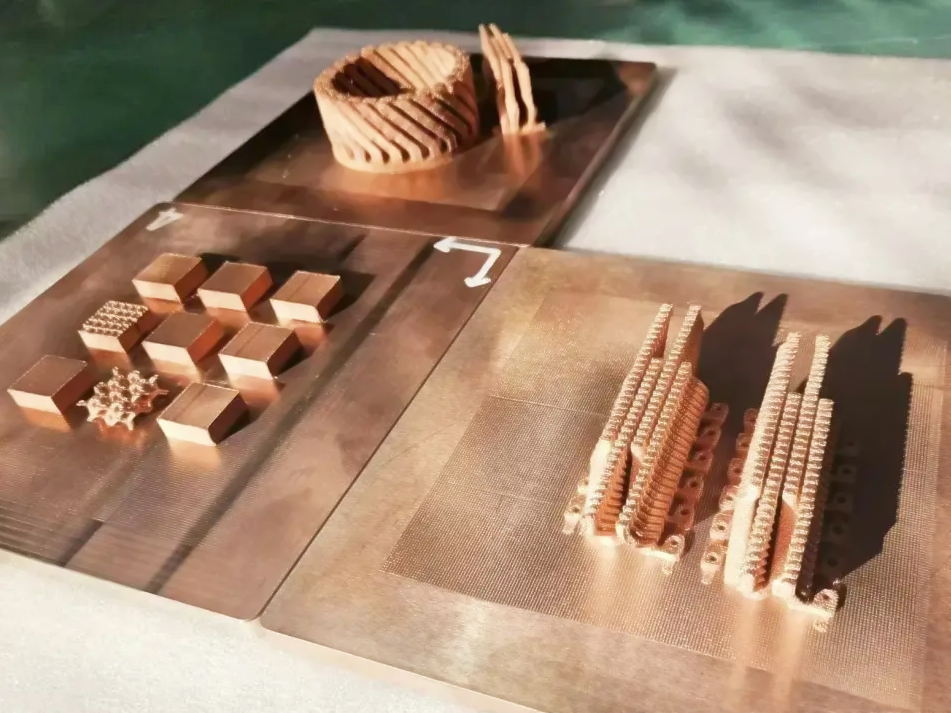
Applications and Industry Case Studies
Copper C101 is widely used in:
Electronics: RF shields, busbars, waveguides, connector housings.
Thermal Management: Cold plates, heat exchangers, cooling fins for high-power electronics.
Aerospace: Antenna components, power distribution systems, EMI shielding.
Medical: Custom electrical contacts and biocompatible thermal devices.
Case Study: RF waveguide prototypes 3D printed using DMLS and post-polished achieved >98% IACS conductivity and dimensional stability for aerospace communications systems.
Frequently Asked Questions (FAQs)
How does Copper C101 maintain conductivity after 3D printing?
Which applications benefit most from C101 copper additive manufacturing?
What post-processing is required for printed C101 copper parts?
What is the typical density and conductivity achieved in DMLS copper printing?
How does Copper C101 compare with C110 and GRCop-42 in electronics?
Explore Related Blogs