Copper C110
Introduction to Copper C110 for 3D Printing
Copper C110, or Electrolytic Tough Pitch (ETP) copper, contains a minimum of 99.90% pure copper and is valued for its high electrical conductivity (~100% IACS) and excellent thermal conductivity (386 W/m·K). It is widely used in power distribution, electronics, and heat management systems.
Through Direct Metal Laser Sintering (DMLS) and Electron Beam Melting (EBM), C110 copper parts achieve precision tolerances of ±0.1 mm while maintaining critical conductive and thermal properties.
International Equivalent Grades of Copper C110
Country | Grade Number | Other Names/Titles |
|---|---|---|
USA | C11000 | ETP Copper |
Europe | CW009A | EN 13601 |
UK | C110 | BS EN 12163 |
China | T2 | GB/T 5231 |
Japan | C1100 | JIS H3100 |
Comprehensive Properties of Copper C110
Property Category | Property | Value |
|---|---|---|
Physical | Density | 8.94 g/cm³ |
Melting Point | 1,083°C | |
Thermal Conductivity | 386 W/m·K | |
Electrical Conductivity | ~100% IACS | |
Chemical | Copper (Cu) | ≥99.90% |
Oxygen (O₂) | ≤0.04% | |
Mechanical | Tensile Strength | 210 MPa |
Yield Strength | 70 MPa | |
Elongation | ≥30% | |
Hardness (Vickers HV) | ~45 HV |
Suitable 3D Printing Processes for Copper C110
Process | Typical Density Achieved | Surface Roughness (Ra) | Dimensional Accuracy | Application Highlights |
|---|---|---|---|---|
≥98% | 10-14 µm | ±0.1 mm | High-precision conductive parts, excellent for thermal/electrical integration in compact assemblies | |
≥99.5% | 20-30 µm | ±0.15 mm | Ideal for large copper heat exchangers and complex high-power electrical fittings |
Selection Criteria for Copper C110 3D Printing Processes
Electrical Conductivity: DMLS retains 95–98% IACS in final parts, essential for current-carrying structures, circuit terminations, and RF shielding.
Thermal Performance: EBM is preferred for thermal components due to minimal oxidation, preserving thermal conductivity near 386 W/m·K.
Surface Precision: DMLS offers fine detail printing; CNC finishing reduces Ra below 1 µm for contact-critical features.
Size and Volume: DMLS suits small precision parts; EBM supports high-volume, large copper components with consistent density.
Essential Post-Processing Methods for Copper C110 3D Printed Parts
Heat Treatment: Conducted at 400–500°C to improve grain structure, reduce residual stress, and restore ductility for cold-worked surfaces.
CNC Machining: Provides fine finish and tight tolerance (±0.02 mm), critical for busbars, connector housings, and EMI interfaces.
Electropolishing: Enhances surface smoothness and conductivity, bringing Ra below 0.5 µm, ideal for electronics and thermal management.
Tumbling: Mechanical finishing method to remove burrs and prep surfaces prior to coating or assembly.
Challenges and Solutions in Copper C110 3D Printing
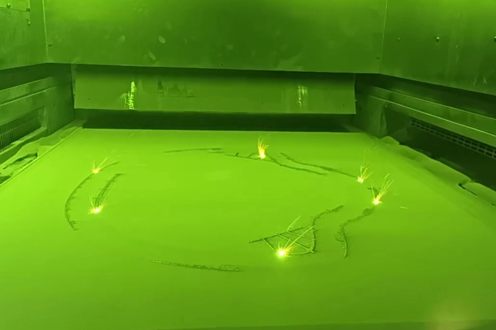
Reflectivity and Laser Absorption: DMLS requires specialized green or blue lasers for stable melting; EBM avoids this issue via electron beam absorption.
Oxidation Sensitivity: Controlled argon atmosphere or vacuum printing is mandatory to avoid oxygen contamination and conductivity reduction.
High Heat Conductivity: Efficient heat dissipation during printing requires optimized scan strategies to ensure melt pool consistency and bonding.
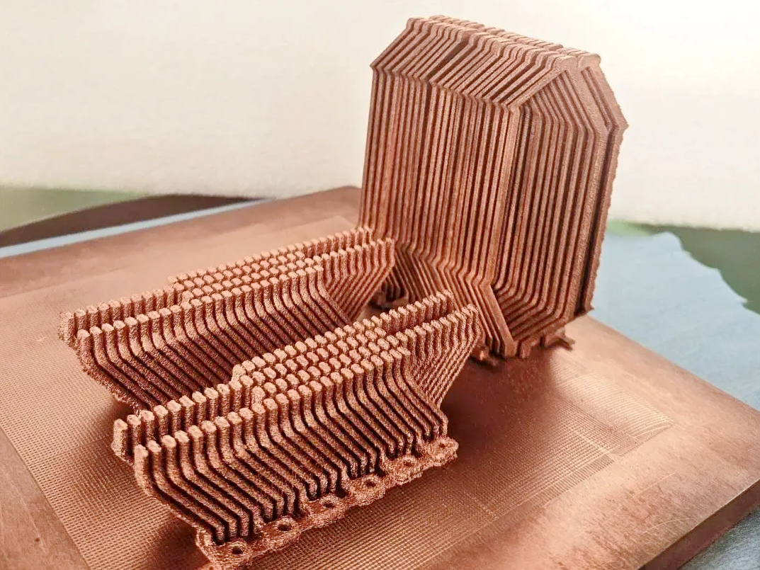
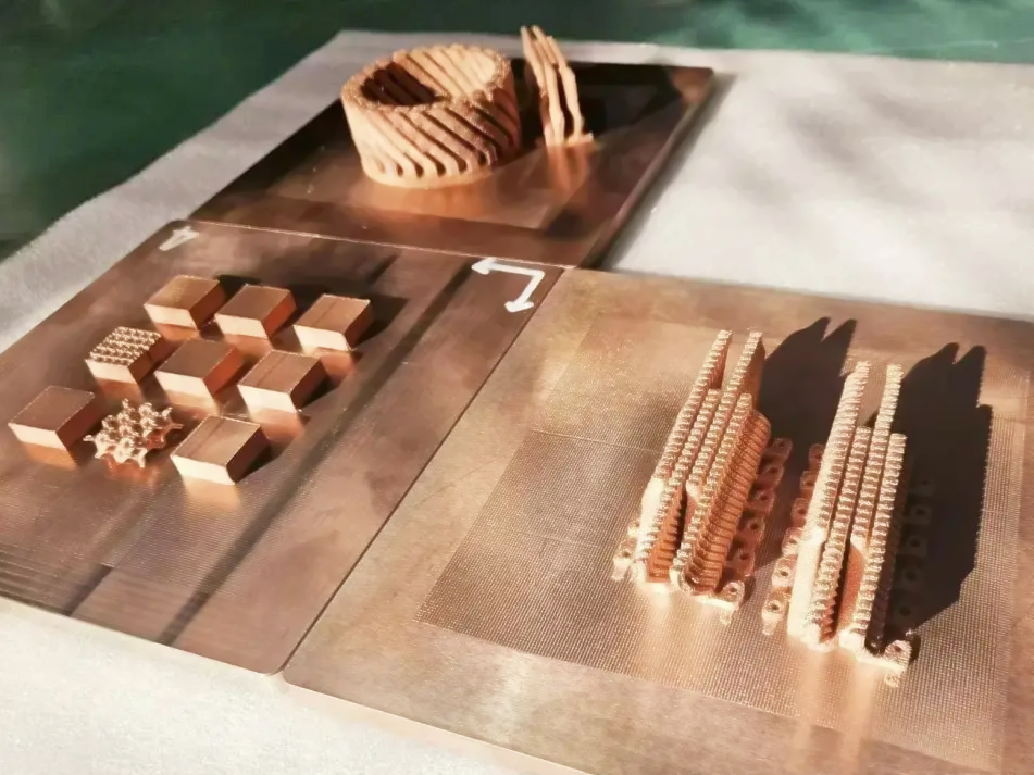
Applications and Industry Case Studies
Copper C110 is widely used in:
Electronics: Grounding conductors, busbars, RF connectors, signal shielding structures.
Power Systems: Current-carrying components, motor terminals, switchgear parts.
Thermal Control: Cold plates, passive heatsinks, high-efficiency radiator segments.
Aerospace & Defense: EMI/RF enclosures, waveguides, radar components.
Case Study: A custom C110 3D printed RF shielding cage was produced using DMLS and electropolished, resulting in conductivity >96% IACS and precise geometry fitment within ±0.08 mm.
Frequently Asked Questions (FAQs)
What conductivity can be expected from 3D printed Copper C110 parts?
Which 3D printing methods are optimal for C110 copper applications?
How is surface quality and electrical contact achieved in C110 components?
Is post-processing necessary to restore full IACS conductivity after printing?
How does Copper C110 compare to C101 and GRCop-42 in high-frequency environments?
Explore Related Blogs