Pure Copper
Introduction to Pure Copper for 3D Printing
Pure copper (≥99.95% Cu) provides unmatched thermal conductivity (~390–400 W/m·K) and electrical conductivity (>100% IACS), making it indispensable in RF shielding, heat exchangers, busbars, and electrical contacts. However, its high reflectivity and thermal conductivity require advanced additive manufacturing techniques.
Direct Metal Laser Sintering (DMLS) and Electron Beam Melting (EBM) enable precise geometries and conductivity retention when processed in controlled inert or vacuum environments.
International Equivalent Grades of Pure Copper
Country | Grade Number | Other Names/Titles |
|---|---|---|
USA | C11000/C10200 | ETP Copper / OFE Copper |
Europe | CW009A | EN 13601 |
Japan | C1100/C1020 | JIS H3100 |
China | T1/TU1 | GB/T 5231 |
Comprehensive Properties of Pure Copper
Property Category | Property | Value |
|---|---|---|
Physical | Density | 8.94 g/cm³ |
Melting Point | 1,083°C | |
Thermal Conductivity | 390–400 W/m·K | |
Electrical Conductivity | ≥100% IACS | |
Chemical | Copper (Cu) | ≥99.95% |
Oxygen (O₂) | ≤0.001% (for OFE) | |
Mechanical | Tensile Strength | 200–250 MPa |
Yield Strength | 50–70 MPa | |
Elongation | ≥35% | |
Hardness (Vickers HV) | ~45–55 HV |
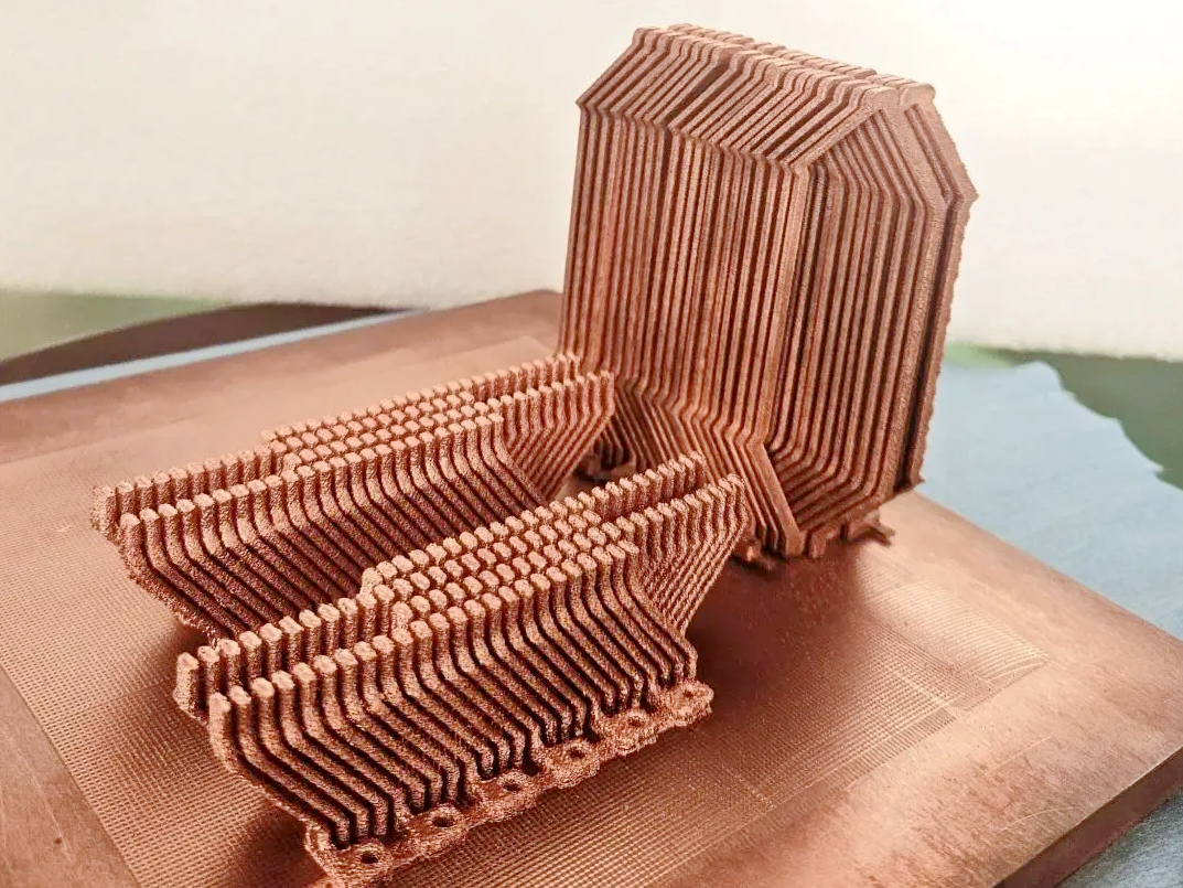
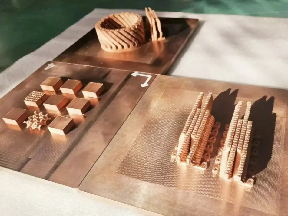
Suitable 3D Printing Processes for Pure Copper
Process | Typical Density Achieved | Surface Roughness (Ra) | Dimensional Accuracy | Application Highlights |
|---|---|---|---|---|
≥98% | 8–12 µm | ±0.1 mm | High-resolution features for electrical and thermal transfer parts | |
≥99.5% | 20–30 µm | ±0.15 mm | Best for large conductive parts requiring low oxide levels |
Selection Criteria for Pure Copper 3D Printing Processes
Conductivity Prioritization: Green laser DMLS achieves >95% IACS; EBM retains full conductivity in large parts due to vacuum processing.
Application Type: Use DMLS for small, detailed electrical contact parts; use EBM for mass thermal systems like cold plates and busbars.
Oxidation Control: Argon (DMLS) or vacuum (EBM) atmospheres are critical to avoid conductivity-degrading oxide layers.
Post-Processing Compatibility: Pure copper is soft and easily machinable. CNC finishing is recommended for sealing surfaces and dimensional control.
Essential Post-Processing Methods for Pure Copper 3D Printed Parts
CNC Machining: Ensures ±0.02 mm tolerance and prepares surfaces for optimal electrical contact and heat transfer interfaces.
Electropolishing: Reduces surface roughness to <0.5 µm Ra, enhancing both conductivity and fatigue resistance for RF or power devices.
Thermal Annealing: Performed at 400–600°C to eliminate residual stress, restore ductility, and improve electrical uniformity.
Tumbling: Used for external surfaces with complex shapes to improve appearance and prepare for coatings or contact finishes.
Challenges and Solutions in Pure Copper 3D Printing
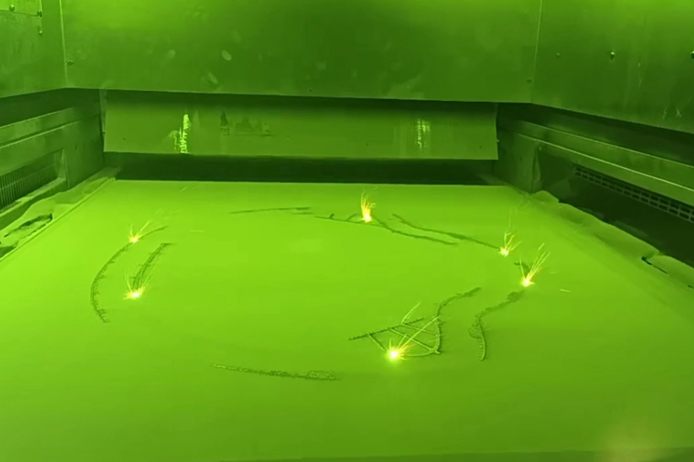
Laser Reflectivity: Specialized green lasers (515–532 nm) are used to maximize energy absorption in DMLS and ensure full melting.
Heat Dissipation During Printing: High thermal conductivity causes premature solidification; tightly controlled layer strategies prevent incomplete fusion.
Oxidation Sensitivity: Printing in environments with <10 ppm oxygen is mandatory to preserve high conductivity and mechanical integrity.
Applications and Industry Case Studies
Pure Copper is widely used in:
Electronics: RF cavities, shielding, connector pins, and signal distribution components.
Power Systems: Busbars, terminal blocks, and high-current carriers.
Thermal Management: Cold plates, heat exchangers, and LED cooling structures.
Aerospace & Defense: Passive thermal control structures, antenna elements, and propulsion interfaces.
Case Study: A 3D printed RF cavity in pure copper achieved >99% IACS conductivity and dimensional accuracy of ±0.08 mm after post-machining and electropolishing, enabling aerospace-grade performance.
Frequently Asked Questions (FAQs)
What conductivity values can be achieved with 3D printed pure copper?
How do DMLS and EBM compare for printing high-purity copper parts?
What post-processing is essential to optimize printed pure copper properties?
What industries benefit most from pure copper additive manufacturing?
How does pure copper compare to GRCop-42 and CuCr1Zr for thermal applications?
Explore Related Blogs