Which 3D printing technology is best for copper parts in electronics applications?
Which 3D Printing Technology Is Best for Copper Parts in Electronics Applications?
Optimal Technology: Selective Laser Melting (SLM) with High-Power Lasers
For functional copper parts in electronics applications, Selective Laser Melting (SLM) is the most effective 3D printing technology. SLM systems equipped with high-power green or infrared lasers can successfully process pure copper and high-conductivity copper alloys, such as Copper C101 and Copper C110, which are widely used in electrical and thermal systems.
SLM is preferred because it enables high-density, fully fused copper parts with excellent electrical conductivity (>90% IACS) and thermal conductivity (>380 W/m·K), meeting the performance needs of advanced electronics.
Why SLM Is Preferred for Copper in Electronics
High laser absorptivity at shorter wavelengths (green laser) improves fusion quality for copper’s reflective surface.
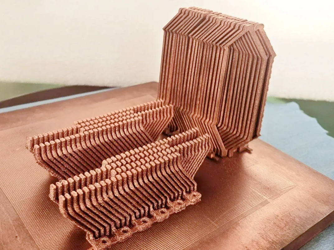
Achieves over 98% relative density with low internal porosity.
Supports complex geometries such as conformal cooling channels and embedded conductor paths.
Maintains critical tolerances for thin walls and compact electronic enclosures.
Applications in Electronics
SLM-printed copper is used in:
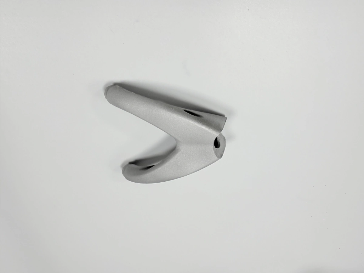
RF and microwave waveguides
Inductors, antennas, and EMI shielding
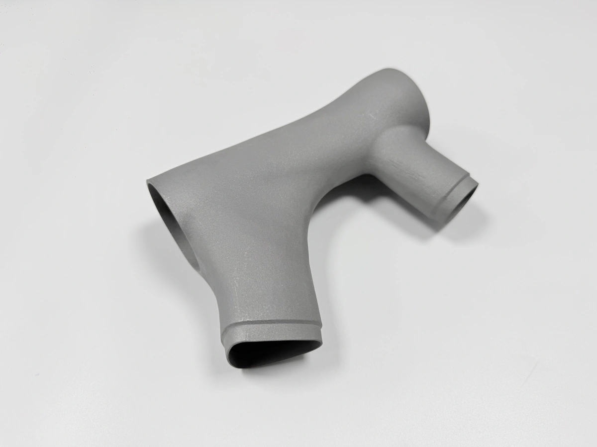
Heat exchangers and cold plates
Electrical bus bars and connector housings
Conformal coils and winding assemblies for sensors and actuators
Customer-Oriented Solutions and Services
To support copper part production for electronics, we offer:
3D Printing Technologies:
Utilize Copper Alloy 3D Printing based on SLM for precision electrical and thermal performance.
Copper Material Selection:
Choose from Copper C101, Copper C110, and CuCr1Zr based on conductivity, strength, and form factor requirements.
Electronics Industry Solutions:
Explore our consumer electronics and energy and power applications, supported by CNC machining and surface treatment for post-processing and performance tuning.