Does three-dimensional printed copper match traditional thermal and electrical conductivity?
Does 3D Printed Copper Match Traditional Thermal and Electrical Conductivity?
Thermal Conductivity Comparison
Copper produced by traditional methods, such as forging or rolling, typically achieves thermal conductivity values around 390–400 W/m·K for high-purity grades like C101. With optimized process parameters, 3D printed copper, particularly using Direct Metal Laser Sintering (DMLS) and Electron Beam Melting (EBM), can reach 85–95% of this conductivity, depending on part density and post-processing.
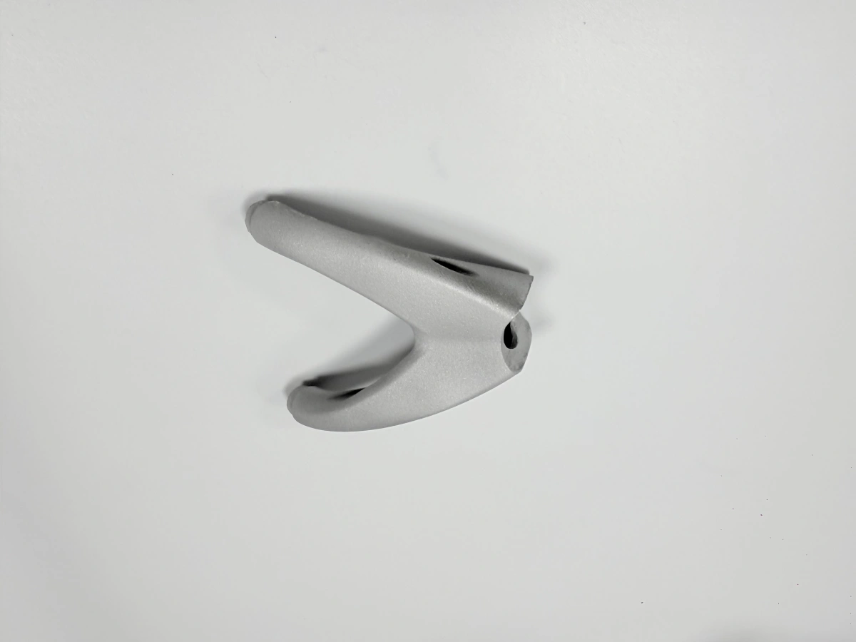
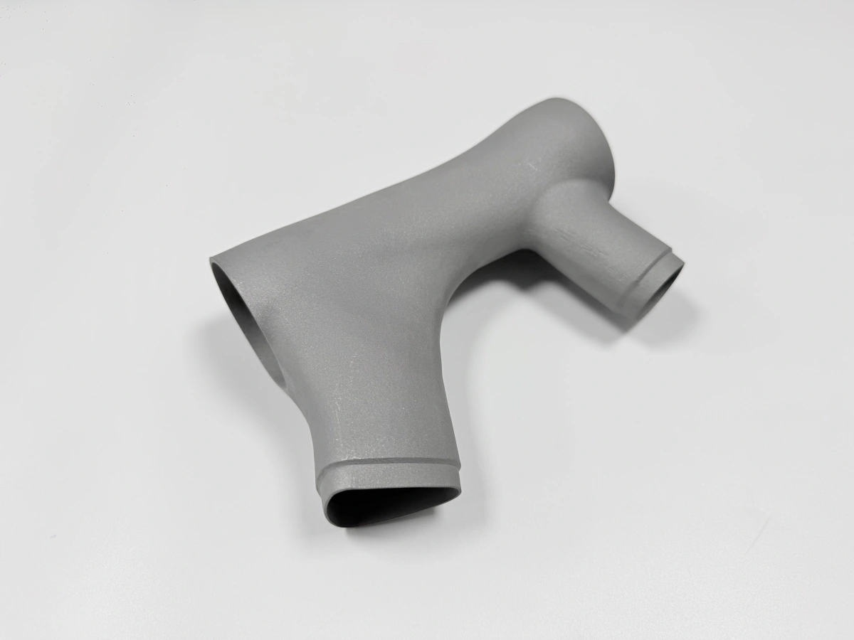
At Neway, printed copper parts using Copper C101 or Pure Copper achieve thermal conductivity values in the range of 340–370 W/m·K after densification and finishing treatments such as Hot Isostatic Pressing (HIP), making them suitable for demanding applications such as heat exchangers and thermal management systems in aerospace and electronics.
Electrical Conductivity Considerations
Wrought copper, especially grades like C110 and C101, typically exhibits electrical conductivity up to 100% IACS (International Annealed Copper Standard). In contrast, 3D printed copper parts without additional densification or heat treatment may initially reach 70–85% IACS due to residual porosity and microstructural imperfections.
However, by using advanced processes such as EBM, combined with post-process treatments like annealing, Neway’s Copper C110 and GRCop-42 parts consistently exceed 90% IACS, aligning with high-performance electrical requirements for power distribution, EMI shielding, and RF components.
Microstructure and Density Optimization
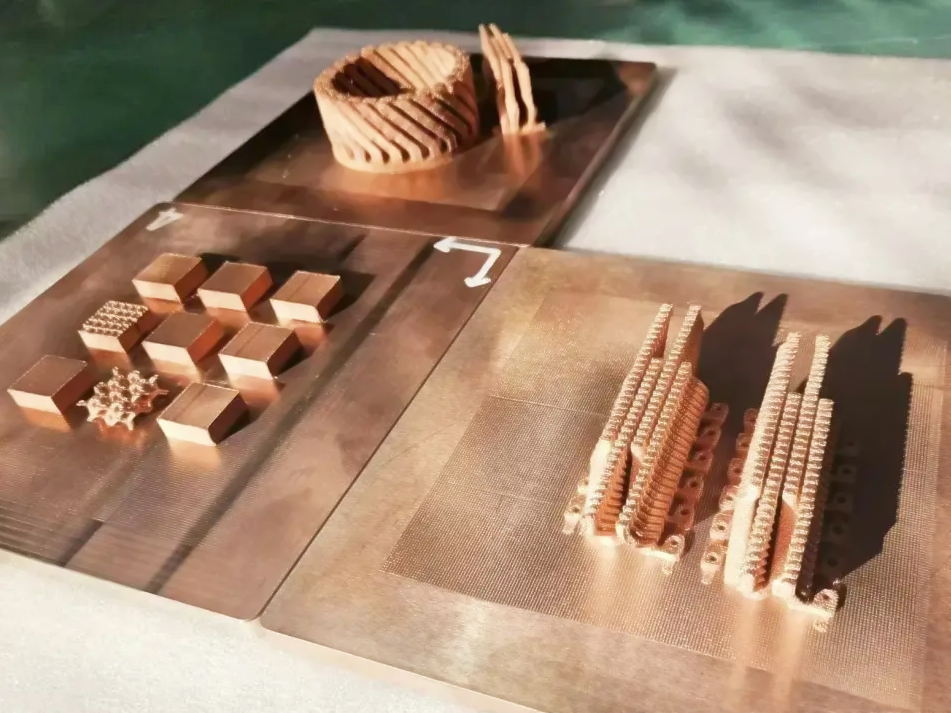
Microstructural refinement plays a critical role in conductivity performance. At Neway, powder selection, layer thickness optimization, and laser scanning strategies are specifically tuned to ensure minimal porosity (typically <1%) and grain boundary control. When paired with electropolishing and surface treatment, surface resistance and thermal barrier interfaces are also minimized, which is critical for high-current applications.
Recommended Copper 3D Printing Solutions at Neway
Copper Alloy 3D Printing: Access high-conductivity materials like Copper C101, Copper C110, and Pure Copper, optimized for thermal and electrical performance.
Thermal and Electrical Performance Post-Treatment: Enhance density and conductivity with HIP, heat treatment, and electropolishing.
Precision Applications Engineering: Get expert guidance for applications requiring strict thermal/electrical performance in sectors like energy and power, aerospace, and consumer electronics.