Silicon Carbide (SiC)
Silicon Carbide (SiC) is an advanced ceramic material renowned for its extreme hardness, thermal conductivity, and resistance to high temperatures and corrosive environments. It is ideal for applications involving abrasive wear, thermal shock, and chemical exposure.
Using ceramic 3D printing, SiC enables the fabrication of complex, lightweight, and high-performance parts such as nozzles, heat exchangers, seal rings, and semiconductor fixtures—components often impossible to produce with conventional manufacturing.
Silicon Carbide Similar Grades Table
Grade Type | Purity (%) | Typical Applications |
|---|---|---|
Reaction-Bonded SiC (RB-SiC) | 88–92 | Burner nozzles, heat exchangers |
Sintered SiC (SSiC) | ≥99 | Mechanical seals, semiconductor tools |
Hot-Pressed SiC (HP-SiC) | ≥99.5 | Optics, structural armor |
Silicon Carbide Comprehensive Properties Table
Category | Property | Value |
|---|---|---|
Physical Properties | Density | 3.10–3.21 g/cm³ |
Melting Point (sublimes) | ~2700°C | |
Thermal Conductivity (25°C) | 120–200 W/(m·K) | |
Electrical Resistivity (25°C) | 10⁵–10¹¹ Ω·cm | |
Thermal Expansion (25–1000°C) | 4.0 µm/(m·K) | |
Mechanical Properties | Hardness (Vickers) | 2500–2800 HV |
Flexural Strength | 400–600 MPa | |
Compressive Strength | ≥2000 MPa | |
Elastic Modulus | 400–450 GPa | |
Fracture Toughness (K₁C) | 3–4.5 MPa·m½ |
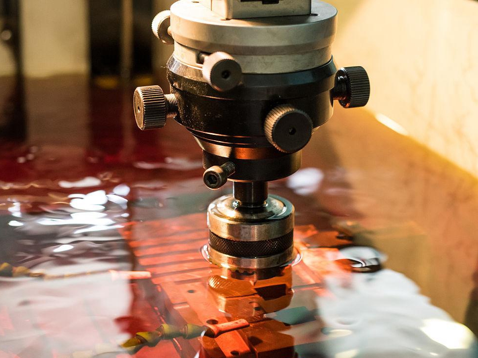
3D Printing Technology of Silicon Carbide
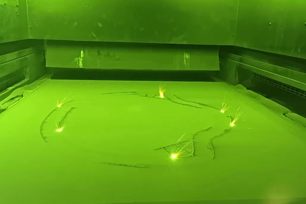
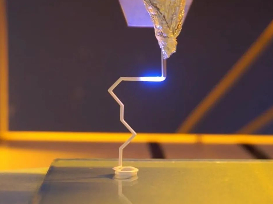
SiC is typically 3D printed via Binder Jetting, with some emerging Vat Photopolymerization (VPP) and laser-based methods under development. Post-printing requires debinding, infiltration or sintering, and often siliconization in reaction-bonded processes.
Applicable Process Table
Technology | Precision | Surface Quality | Mechanical Properties | Application Suitability |
|---|---|---|---|---|
Binder Jetting | ±0.1–0.3 mm | Good | Good–Very Good | Heat Exchangers, Tooling Fixtures |
Vat Photopolymerization (VPP) | ±0.05–0.2 mm | Excellent | Good | Fine Flow Channels, Sensors |
Hybrid Si Infiltration | ±0.1–0.3 mm | Good | Excellent | Reaction-Bonded SiC Parts |
Silicon Carbide 3D Printing Process Selection Principles
Binder Jetting is preferred for larger, geometrically complex parts such as heat exchangers and kiln furniture, with cost-effective batch production and excellent thermal performance after sintering or infiltration.
VPP is suitable for high-precision SiC microstructures, enabling internal channels or thin-walled geometries in applications like flow reactors and infrared optics.
Reaction-bonded SiC using 3D printed green bodies and molten silicon infiltration yields strong, dense components suitable for semiconductor and energy equipment.
Silicon Carbide 3D Printing Key Challenges and Solutions
SiC is extremely hard but brittle, making debinding and sintering stages critical. Controlled heating rates (≤2–3°C/min) and atmosphere control during processing reduce crack formation.
Shrinkage (15–25%) and warping during sintering can be managed through precise CAD scaling and uniform thermal gradients. Final parts typically achieve >97% theoretical density.
Surface finish (Ra 8–15 µm) impacts sealing and flow performance. Post-processing such as diamond polishing, lapping, or infiltration improves strength and aesthetics, achieving Ra < 1.5 µm.
Oxygen-sensitive sintering or infiltration processes require inert or vacuum atmospheres to prevent defect formation and achieve complete densification.
Industry Application Scenarios and Cases
Silicon Carbide 3D printing is used in:
Semiconductor: Etching chambers, wafer handling, high-purity supports.
Energy: Gas burner nozzles, heat exchanger fins, and combustion liners.
Aerospace: Lightweight, high-stiffness thermal shields and mirror blanks.
Industrial: Seal rings, wear plates, mixer blades, and abrasive tooling.
In a recent energy sector project, binder jet printed SiC burner nozzles showed 40% weight savings and extended service life over cast components, performing reliably at 1500°C under cyclic loading.
FAQs
What are the benefits of Silicon Carbide over Alumina in extreme environments?
Which 3D printing technologies are suitable for SiC fabrication?
How is post-processing handled for 3D printed SiC components?
What industries benefit most from Silicon Carbide additive manufacturing?
How does binder jetting compare to infiltration-based SiC 3D printing?
Explore Related Blogs