Alumina (Al2O3)
Alumina (Al₂O₃) is a high-purity oxide ceramic known for exceptional hardness, electrical insulation, and thermal resistance. It is widely used in electronics, aerospace, medical, and industrial applications requiring dimensional stability and wear performance under extreme conditions.
With advanced ceramic 3D printing, Alumina can be manufactured into complex, high-precision components, including insulators, nozzles, and biomedical tools. Additive manufacturing enables small-batch customization, lightweight structures, and internal channels that are impossible with traditional forming methods.
Alumina Similar Grades Table
Grade | Purity (%) | Typical Applications |
|---|---|---|
96% Alumina | ≥96 | Electrical insulators, wear plates |
99% Alumina | ≥99 | Semiconductor components, substrates |
99.8% High-Purity | ≥99.8 | Medical implants, analytical instruments |
Alumina Comprehensive Properties Table
Category | Property | Value |
|---|---|---|
Physical Properties | Density | 3.85–3.98 g/cm³ |
Melting Point | ~2050°C | |
Thermal Conductivity (25°C) | 25–35 W/(m·K) | |
Electrical Resistivity (25°C) | >10¹⁴ Ω·cm | |
Thermal Expansion (25–1000°C) | 7.5–8.5 µm/(m·K) | |
Mechanical Properties | Hardness (Vickers) | 1500–2000 HV |
Flexural Strength | 300–400 MPa | |
Compressive Strength | ≥2000 MPa | |
Elastic Modulus | 300–400 GPa | |
Fracture Toughness (K₁C) | 3–4 MPa·m½ |
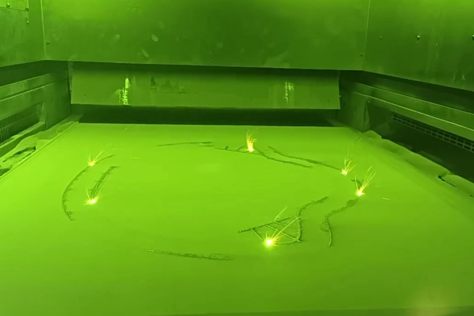
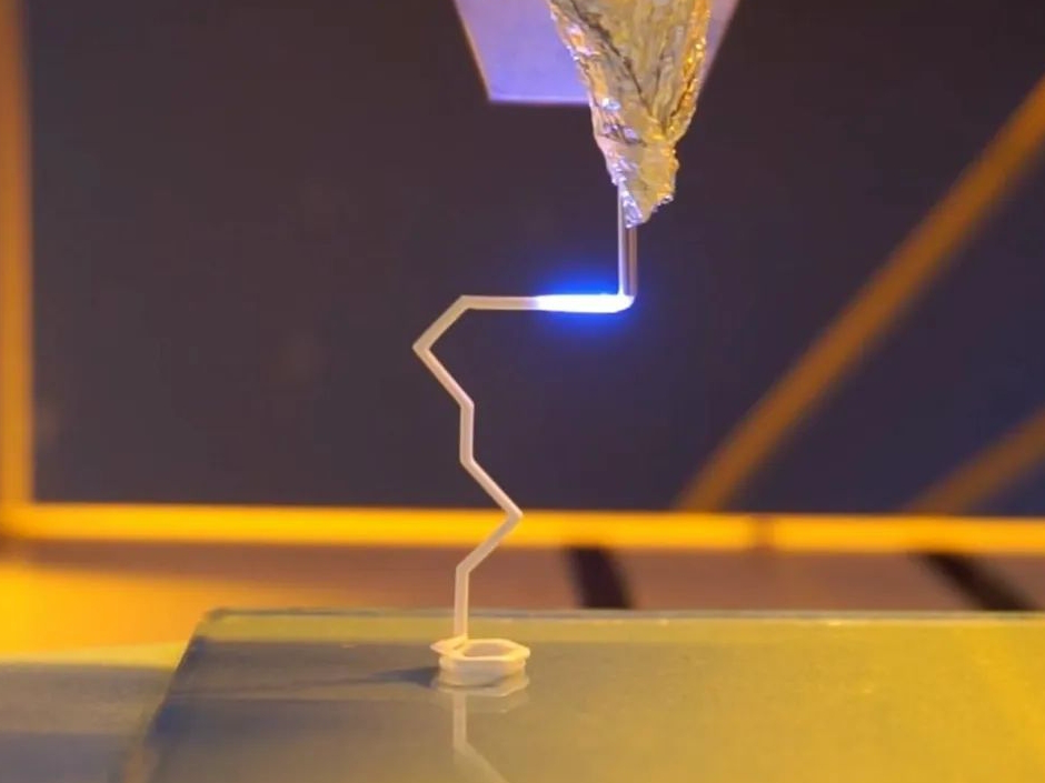
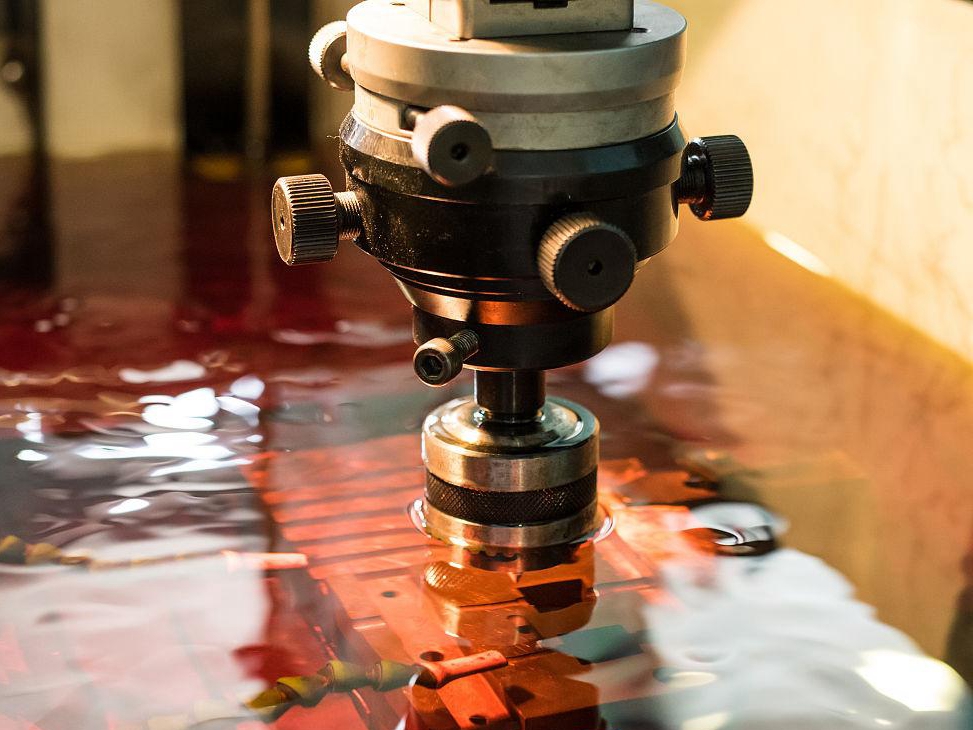
3D Printing Technology of Alumina
Alumina is typically 3D printed using Vat Photopolymerization (VPP), Material Jetting, and Binder Jetting methods, followed by debinding and sintering. These technologies achieve tight tolerances and fine feature resolution for functional ceramic parts.
Applicable Process Table
Technology | Precision | Surface Quality | Mechanical Properties | Application Suitability |
|---|---|---|---|---|
Vat Photopolymerization (VPP) | ±0.05–0.2 mm | Excellent | Excellent | Medical, Aerospace, Electronics |
Material Jetting | ±0.1–0.3 mm | Very Good | Good | Insulators, Wear Components |
Binder Jetting | ±0.1–0.3 mm | Good | Moderate | Structural, Large-Scale Ceramics |
Alumina 3D Printing Process Selection Principles
VPP is preferred for high-precision ceramic parts such as microfluidic chips, biomedical guides, and electrical isolators requiring Ra < 2 µm and tolerances of ±0.05–0.2 mm.
Material Jetting is suitable for smooth-surfaced electrical insulators, substrates, and biomedical parts requiring surface detail and moderate complexity.
Binder Jetting supports large-format ceramic components and offers a cost-effective solution for prototyping or tooling, with good mechanical strength after sintering.
Alumina 3D Printing Key Challenges and Solutions
Shrinkage during sintering is a major challenge. Accurate compensation in CAD design and the use of sintering-resistant support structures ensure dimensional accuracy post-processing.
Porosity impacts strength and electrical performance. Using high-solid loading ceramic resins and optimized sintering cycles improves final density to >98%, ensuring mechanical and dielectric reliability.
Surface roughness and microcracks from thermal gradients are reduced by fine-tuned exposure strategies and post-sinter polishing, achieving surface finishes Ra 0.4–1.0 µm where required.
Alumina powders and slurries must be processed in humidity-controlled environments (RH < 40%) to prevent defect formation during drying and sintering.
Industry Application Scenarios and Cases
Alumina is widely used in:
Electronics: High-voltage insulators, substrates, and semiconductor spacers.
Medical: Bioinert dental prosthetics, surgical guides, and instrument tips.
Aerospace: Wear-resistant bushings, nozzles, and thermal shielding components.
In a recent semiconductor project, VPP 3D printed 99.8% alumina sensor housings were delivered with tolerances under ±0.05 mm and >99% relative density, outperforming traditional pressed parts in dimensional repeatability and lead time.
FAQs
What purity grades of Alumina are suitable for 3D printing applications?
Which ceramic 3D printing technologies are best for producing high-precision Alumina parts?
What post-processing steps are required for Alumina 3D printed components?
How does Alumina 3D printing compare to traditional ceramic forming?
What industries benefit most from Al₂O₃ 3D printed components?
Explore Related Blogs