Copper CuNi2SiCr
Introduction to Copper CuNi2SiCr for 3D Printing
CuNi2SiCr is a precipitation-hardened copper alloy with 1.6–2.5% nickel, 0.5–1.2% silicon, and 0.2–0.8% chromium. It offers a superior balance of electrical conductivity (40–60% IACS), mechanical strength (up to 700 MPa), and wear resistance, making it ideal for high-performance electrical contacts, switch components, and aerospace connectors.
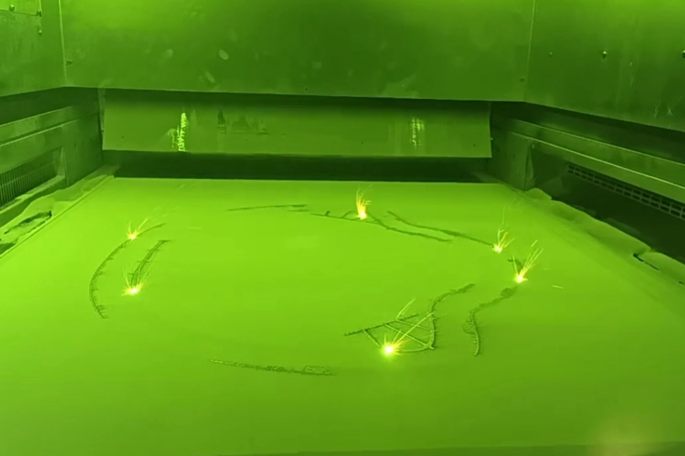
Direct Metal Laser Sintering (DMLS) and Selective Laser Melting (SLM) allow CuNi2SiCr to achieve dimensional accuracy of ±0.05 mm and maintain post-print mechanical integrity and conductivity.
International Equivalent Grades of Copper CuNi2SiCr
Country | Grade Number | Other Names/Titles |
|---|---|---|
USA | C70250 | Alloy 7025 |
Europe | CW111C | EN 1652 |
China | QNi2SiCr | GB/T 2059 |
Japan | C7025 | JIS H3100 |
Comprehensive Properties of Copper CuNi2SiCr
Property Category | Property | Value |
|---|---|---|
Physical | Density | 8.85 g/cm³ |
Melting Point | 1,070–1,085°C | |
Thermal Conductivity | ~200 W/m·K | |
Electrical Conductivity | 40–60% IACS | |
Chemical | Copper (Cu) | Balance |
Nickel (Ni) | 1.6–2.5% | |
Silicon (Si) | 0.5–1.2% | |
Chromium (Cr) | 0.2–0.8% | |
Mechanical | Tensile Strength (aged) | 600–700 MPa |
Yield Strength (aged) | 450–600 MPa | |
Elongation | ≥10% | |
Hardness (Vickers HV) | 140–180 HV |
Suitable 3D Printing Processes for Copper CuNi2SiCr
Process | Typical Density Achieved | Surface Roughness (Ra) | Dimensional Accuracy | Application Highlights |
|---|---|---|---|---|
≥99% | 8–12 µm | ±0.05 mm | Best for high-strength, electrically conductive parts with complex geometries | |
≥99.5% | 6–10 µm | ±0.05 mm | Ideal for aerospace terminals, heat-resistant connectors, and spring contacts |
Selection Criteria for CuNi2SiCr 3D Printing Processes
Strength vs. Conductivity Trade-Off: Post-aging CuNi2SiCr offers 700 MPa strength with up to 60% IACS conductivity—ideal for components under mechanical and electrical load.
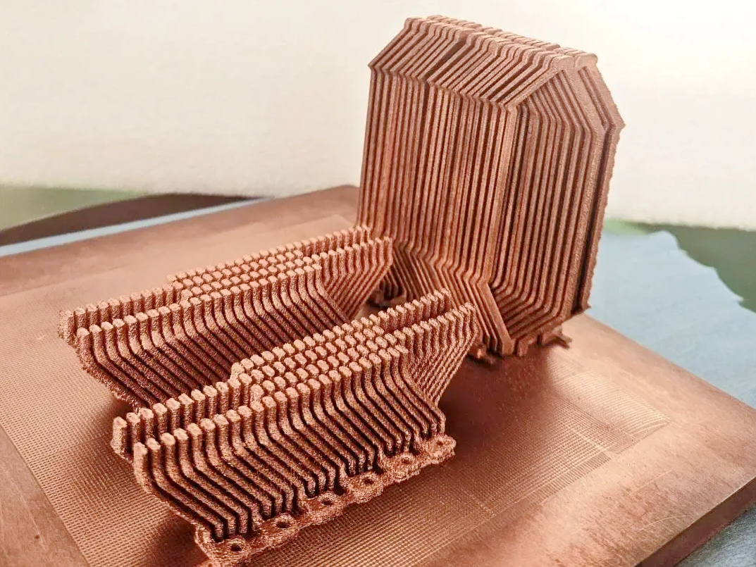
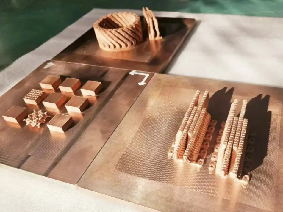
Fine Feature Requirements: DMLS and SLM are suitable for thin-walled structures and intricate contacts where precision is required (<0.4 mm wall thickness).
Thermal and Fatigue Resistance: Its low thermal expansion and high fatigue strength make it excellent for dynamic load applications and thermal cycling environments.
Post-Processing Compatibility: CuNi2SiCr responds well to age hardening and CNC finishing, critical for maintaining contact resistance and geometry.
Essential Post-Processing Methods for CuNi2SiCr 3D Printed Parts
Age Hardening: Aging at 450–480°C for 1–4 hours boosts tensile strength and stabilizes conductivity while refining grain structure.
CNC Machining: Used to achieve tight tolerances (±0.02 mm) and prepare interface surfaces for reliable electrical contact.
Polishing & Electropolishing: Surface finish Ra < 0.5 µm for low-resistance contacts and aesthetically critical visible components.
Shot Peening: Enhances fatigue resistance and surface hardness—ideal for spring connectors and mechanical contacts.
Challenges and Solutions in CuNi2SiCr 3D Printing
Alloy Segregation During Printing: Uniform powder size and optimized scan strategies prevent elemental segregation and maintain homogeneous composition.
Heat Input Management: Controlled energy density avoids overaging or distortion, preserving strength and dimensional accuracy.
Surface Oxide Removal: Post-print electropolishing and cleaning ensure optimal conductivity for electronic or RF functionality.
Applications and Industry Case Studies
CuNi2SiCr is widely used in:
Electronics: High-cycle switches, micro-relays, and electrical spring connectors.
Aerospace: Avionics signal paths, vibration-resistant contact systems, and structural electrical fittings.
Automotive: EV busbar terminals, fuse box connectors, and signal ground lugs.
Telecom & RF: Spring-loaded sockets, thermal relays, and shielding modules.
Case Study: A 3D printed CuNi2SiCr avionics connector achieved 670 MPa tensile strength, 52% IACS conductivity, and consistent performance over 100,000 mechanical cycles in fatigue testing.
Frequently Asked Questions (FAQs)
What is the typical conductivity and strength of CuNi2SiCr after 3D printing and aging?
Which 3D printing process is best for high-precision electrical contacts using CuNi2SiCr?
What finishing methods are recommended for CuNi2SiCr to reduce contact resistance?
Is CuNi2SiCr suitable for high-cycle fatigue applications in 3D printed parts?
How does CuNi2SiCr compare with C18150 and C7025 for electrical connector fabrication?
Explore Related Blogs