Silicon Dioxide (SiO2) 3D Printing: Custom Optics, Semiconductor Wafers & Glass Molding Components
Introduction
Silicon Dioxide (SiO₂) 3D printing delivers unprecedented precision and material performance for applications in optics, semiconductor manufacturing, and glass molding. Using advanced ceramic 3D printing technologies such as Vat Photopolymerization and Binder Jetting, custom Silicon Dioxide (SiO₂) components can be produced with complex geometries, excellent thermal stability, and superior optical clarity.
Compared to traditional fabrication techniques, SiO₂ 3D printing offers faster lead times, greater design flexibility, and reduced material waste, enabling rapid prototyping and production of high-value precision parts.
Applicable Material Matrix
Material | Purity (%) | Flexural Strength (MPa) | Thermal Expansion (×10⁻⁶/K) | Optical Transmission (%) | Max Operating Temp. (°C) |
|---|---|---|---|---|---|
>99.99% | 65–75 | 0.5 (20–300°C) | >90% (UV to IR range) | 1000 | |
>99.9% | 50–65 | 0.55 (20–300°C) | >88% (UV to visible) | 1050 |
Material Selection Guide
Fused Silica SiO₂: Ideal for high-precision optical lenses, waveguides, and semiconductor wafer substrates, offering near-perfect optical transmission and extremely low thermal expansion.
Quartz Glass SiO₂: Suitable for complex glass molding tools, high-temperature insulators, and optical components requiring high purity and excellent dimensional stability.
Process Performance Matrix
Attribute | Silicon Dioxide 3D Printing Performance |
|---|---|
Dimensional Accuracy | ±0.05–0.1 mm |
Density (after sintering) | >99% Theoretical Density |
Minimum Wall Thickness | 0.5–1.0 mm |
Surface Roughness (As-Sintered) | Ra 3–8 μm |
Feature Size Resolution | 100–200 μm |
Process Selection Guide
High Optical Clarity: Fused Silica maintains over 90% light transmission from ultraviolet through infrared ranges, critical for optical systems.
Thermal Stability: Minimal thermal expansion (0.5×10⁶⁻⁶/K) ensures dimensional accuracy in high-temperature environments, essential for semiconductor fabrication and precision molding.
Complex Geometries: Enables fabricating intricate hollow structures, micro-channels, and free-form optics without costly tooling.
Rapid Customization: Accelerates development cycles for custom optics, wafers, and glass molds with tight production tolerances.
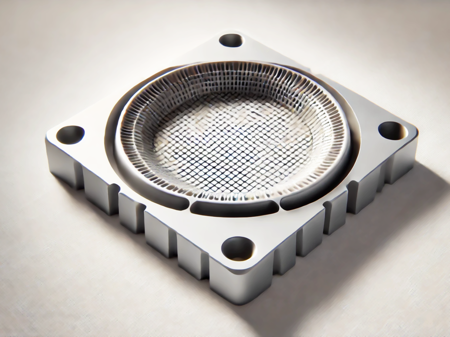
Case In-Depth Analysis: Fused Silica 3D Printed Optics for Semiconductor Lithography
A semiconductor equipment manufacturer needed custom optics with high UV transmission and tight tolerances for next-generation lithography systems. Using our Silicon Dioxide 3D printing service, we fabricated Fused Silica lenses, achieving >90% transmission in the 193 nm UV range, flexural strength over 70 MPa, and dimensional accuracy within ±0.05 mm. Post-processing included precision CNC polishing and surface finishing to achieve surface roughness Ra < 1 μm, ensuring optical-grade performance.
Industry Applications
Optics and Photonics
Custom optical lenses and waveguides.
UV-transparent windows and domes.
Light guides and micro-optical components.
Semiconductor Manufacturing
Fused silica wafer substrates for advanced semiconductor devices.
Reticles and photomasks for lithography systems.
High-temperature process chamber components.
Glass Molding and Tooling
Precision glass molding inserts.
High-temperature molds for optical glass shaping.
Customized tooling for specialty glassware production.
Mainstream 3D Printing Technology Types for Silicon Dioxide Components
Vat Photopolymerization (SLA/DLP): Best for fine-resolution SiO₂ parts requiring smooth surface finishes and intricate details.
Binder Jetting: Ideal for batch production of larger, moderately detailed silicon dioxide components.
Material Extrusion: Suitable for prototyping and larger structural parts requiring robust mechanical strength post-sintering.
FAQs
What are the advantages of using Silicon Dioxide 3D printing for optical applications?
How does 3D printed Fused Silica compare to traditional optical glass components?
What post-processing techniques are used to achieve optical-grade surfaces on SiO₂ parts?
What are the temperature and mechanical limitations of 3D printed Silicon Dioxide parts?
Can 3D printed SiO₂ components match the purity and optical performance required in semiconductor manufacturing?