What are the typical spatial resolution and minimum detectable particle size for SEM/EDS?
Scanning Electron Microscopy coupled with Energy Dispersive X-ray Spectroscopy is a cornerstone technique for materials characterization in additive manufacturing and advanced materials development. Understanding its capabilities and limitations is crucial for effective quality control and research.
Spatial Resolution in SEM/EDS Analysis
SEM Spatial Resolution
The spatial resolution in SEM refers to the smallest distance between two points that can be distinctly visualized. For secondary electron imaging, modern field-emission gun SEMs can achieve resolutions of 1 nm or better at high vacuum. Backscattered electron imaging typically offers slightly lower resolution, ranging from 2 to 5 nm, but provides superior atomic number contrast.
EDS Spatial Resolution
The spatial resolution for EDS is fundamentally different and significantly larger than that of SEM imaging. It is governed by the interaction volume of the electron beam with the sample, from which X-rays are generated. This volume depends on the beam energy and the sample's atomic number.
At 15 kV accelerating voltage: The resolution is approximately 1-2 micrometers.
At 5 kV accelerating voltage: The resolution can be improved to around 0.5-1 micrometer.
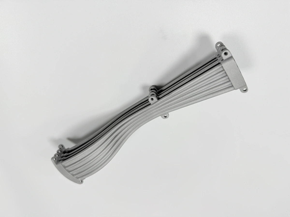
For high-precision analysis of fine features in materials, such as those produced by our Powder Bed Fusion process, using a lower accelerating voltage can help localize the analysis better.
Minimum Detectable Particle Size for EDS
The minimum detectable particle size is not a fixed value but depends on several factors:
Particle Composition: A pure element particle is easier to detect than a compound particle.
Matrix Composition: A heavy element particle on a light element matrix (e.g., a tungsten inclusion in a carbon substrate) is far easier to detect than the reverse.
Beam Energy and Probe Current: Higher beam currents increase X-ray generation, improving the signal from small particles.
As a practical guideline, EDS can reliably identify and analyze particles down to a size similar to its spatial resolution, typically 0.1 to 0.5 micrometers (100 to 500 nanometers) in diameter under optimized conditions. For definitive phase identification of particles near this lower limit, complementary techniques like our CNC Machining service for cross-sectioning may be required to prepare ideal samples.
Application in Additive Manufacturing and Material Science
The capabilities of SEM/EDS are integral to our post-process quality control. For instance, we use it to inspect the microstructure of Titanium Alloy parts, such as Ti-6Al-4V, ensuring there are no undesirable interstitial phases. It is also vital to examine the integrity of Thermal Barrier Coatings (TBCs) and the elemental composition of high-performance Superalloy components used in the Aerospace and aviation industries.
Furthermore, EDS is used to verify the composition of raw material powders, such as those for Aluminum Alloys and Stainless Steel, ensuring they are free from contaminant particles that could compromise the final part's mechanical properties. This level of scrutiny supports applications in demanding sectors, such as medical and Healthcare for implants and Automotive for high-stress components.
To achieve the best sample surface for such high-resolution analysis, a high-quality Surface Treatment is often a critical preparatory step. For analyzing the elemental distribution in complex Ceramic parts or the uniformity of a Copper heat exchanger's internal structure, EDS mapping provides invaluable data.